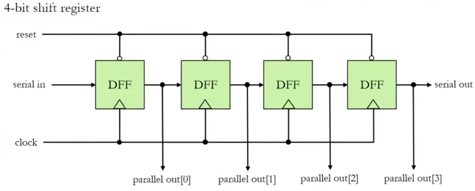
A shift register is formed by connecting flip-flops in series.
Data is shifted through the flip-flops on every clock pulse.
For a 4-bit shift register, it takes 4 clock cycles to fully load 4 bits.
Types
-
SISO (Serial In Serial Out)
- Data is loaded serially (one bit at a time).
- Data is read serially from the last flip-flop.
- Can be used as a buffer or queue in a circuit.
-
SIPO (Serial In Parallel Out)
- Data is loaded serially.
- Data is read in parallel from each flip-flop output.
- Useful when limited pins are available to read a large amount of data.
Shift vs Write Mode
A SW control pin can switch between shift and write mode:
Shift Mode (SW == 1) |
Write Mode (SW == 0) |
|---|---|
| The output of the last flip-flop is fed back into the first flip-flop. | New data is written, but data after the output is lost. |
Block Diagram
Verilog Implementation
module S_Reg(
    input clk, reset, SW, Din,
    output Sout,
    output [7:0] Pout
);

    reg [7:0] SReg; // Internal storage (flip-flops)
    wire Sin;

    // Select between feedback (shift) or new data (write)
    assign Sin = (SW) ? SReg[7] : Din;

    // Shift register logic
    always @(posedge clk or negedge reset) begin
        if (!reset)
            SReg <= 8'd0;
        else
            SReg <= {SReg[6:0], Sin};  // Shift left and insert Sin
    end

    // Outputs
    assign Sout = SReg[7]; // Serial output (last bit)
    assign Pout = SReg;    // Parallel output (all bits)

endmodule