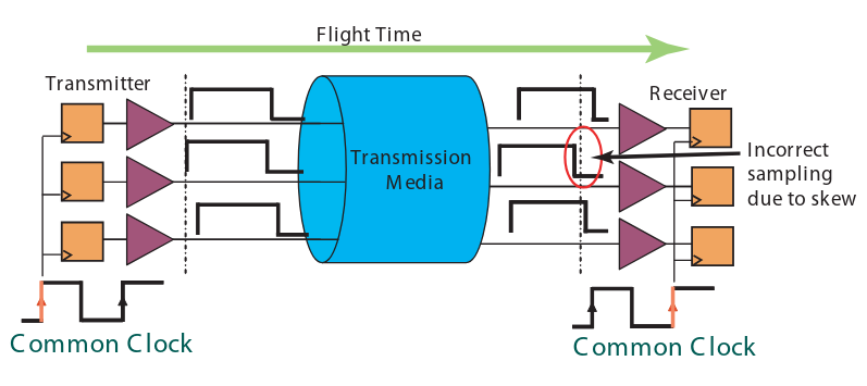
The Common Clock Parallel Bus Model
- All devices on the bus share one global clock (distributed clock).
- Data is launched on one edge (say rising edge) and must be valid and stable by the next edge for the receiver to latch it.
- This means the entire timing budget = one clock period.
👉 At low frequencies (33–66 MHz), this is manageable. But as frequency goes up (100–133 MHz for PCI-X), the timing margin shrinks drastically.
Problems with Scaling Parallel Common Clock
-
Signal Skew (data skew)
- Many bits (AD[31:0], control lines, etc.) travel in parallel.
- Each trace has slightly different length / capacitance / impedance, so signals don’t arrive at the receiver at the same time.
- If the skew is larger than the setup/hold margin, the wrong data gets latched.
-
Clock Skew (device-to-device mismatch)
- The common clock doesn’t reach all devices at exactly the same time.
- Example: Device A might see the clock edge 200 ps earlier than Device B.
- This reduces the effective timing budget, because some devices latch too early or too late relative to the data arrival.
-
Flight Time (propagation delay)
- The electrical signal needs time to physically travel down the PCB trace (roughly 150–180 ps per inch).
- At high frequencies, this flight time eats into the timing budget.
- Designers have to keep traces very short and length-matched, which isn’t always practical when many slots/devices are involved.
👉 Together, these make it nearly impossible to push PCI beyond 133 MHz, even though the theoretical protocol could run faster.
Workarounds Attempted
-
Streamlining the Protocol
- PCI-X reduced idle cycles, improved bursting, added split transactions.
- This improves efficiency but doesn’t solve the underlying clocking issue.
-
Source Synchronous Clocking (PCI-X 2.0 and beyond)
- Instead of distributing one global clock, the transmitter sends its own strobe along with the data.
- Both travel the same path → same propagation delay → no skew between data and clock.
- This allows higher clock rates (266 MHz, 533 MHz in PCI-X 2.0).