- Instead of one common clock shared by all devices (old PCI/PCI-X 1.0),
→ the transmitter sends a strobe signal alongside the data. - Both data and strobe travel the same physical path (same trace length, same delay).
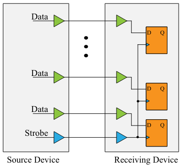
- At the receiver:
- The strobe is used directly to latch the incoming data.
- This removes the uncertainty of clock skew and flight time delays.
✅ Result: The timing margin no longer shrinks when frequency increases → allows very high speeds.
Data Rates Supported
- DDR (Dual Data Rate): Data captured on both edges of the strobe → 2× throughput.
- QDR (Quad Data Rate): Data captured 4× per strobe cycle → 4× throughput.
- Bandwidth increased massively compared to PCI-X 1.0 (133 MHz). PCI-X 2.0 could reach 533 MHz effective speeds.
Why It Works Better
- No clock skew budget → the strobe and data arrive together.
- Flight time irrelevant → as long as both travel the same distance, the relative timing is preserved.
- High-speed friendly → this is why you see similar ideas in DDR SDRAM and HyperTransport.
Limitations Introduced
-
No shared-bus possible anymore
- At such high frequencies, you can’t have multiple devices hanging off the same parallel bus.
- Must be point-to-point connections.
- More devices → more bridges → higher cost.
-
Complex device design
- A single device with 3 buses would need:
- 3 full interfaces
- An internal bridge
- Very high pin count
- Expensive silicon → targeted only at high-end servers/workstations.
- A single device with 3 buses would need:
Reliability Features
As PCI-X recognizes itself to high end market:
- ECC (Error Correcting Code) added on top of parity.
- Can correct single-bit errors on the fly.
- Detects multi-bit errors robustly.
- Important for enterprise servers, where uptime and reliability matter more than cost.