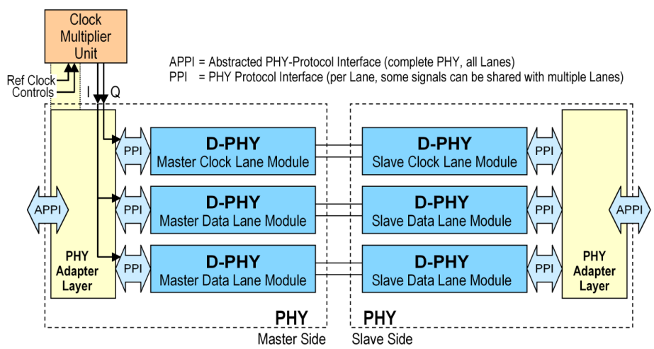
A complete D-PHY Link includes:
- One Clock Lane Module
- One or more Data Lane Modules
- A Clock Multiplier Unit (for high-frequency clock generation)
- A PHY Adapter Layer that connects all lanes and interfaces with the protocol layer
The PHY Adapter Layer coordinates the behavior of the lanes and the clock multiplier, but its internal structure is not defined by this specification.
PHY-Protocol Interface (PPI)
Each Lane provides a logical PHY-Protocol Interface (PPI), which consists of:
- Control signals for managing lane operations
- Data input/output signals appropriate to the lane type (Clock or Data)
Some key points:
- Clock-related control signals can be shared among multiple lanes.
- The reference clock and control signals for the Clock Multiplier Unit are outside the scope of this specification.