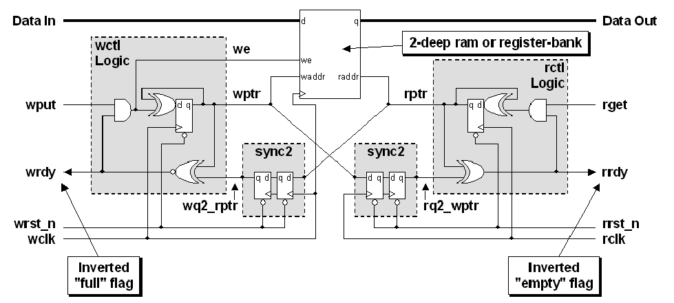
This design is a minimal asynchronous FIFO, optimized for low latency and safe multi-bit transfer between two asynchronous clock domains — without the complexity of full pointer-based FIFOs.
1️⃣ Core Concept
Unlike a traditional FIFO (which might hold many data words),
a 1-deep, 2-register FIFO can only hold one data/control word at a time.
- It consists of two storage elements (registers or a 2-entry dual-port RAM).
- The write domain controls one side of the FIFO.
- The read domain controls the other.
- Each side maintains its own 1-bit pointer — implemented as a toggle flip-flop.
Because there are only two entries, a 1-bit counter (toggle) is sufficient to distinguish between the two storage locations.
2️⃣ FIFO State Machine
| Condition | FIFO Status | Write Ready (wrdy) |
Read Ready (rrdy) |
|---|---|---|---|
| Both pointers equal | Empty | ✅ High (can write) | ❌ Low (no data yet) |
| Pointers different | Full | ❌ Low (cannot write) | ✅ High (data ready) |
- On reset, both pointers = 0 → FIFO empty,
wrdy = 1,rrdy = 0. - When data is written, the write pointer toggles → FIFO becomes full.
- Once the data is read, the read pointer toggles → FIFO becomes empty again.
3️⃣ Operation Flow
Let’s go through the send/receive sequence step by step:
Write Clock Domain (Sender)
wrdy= 1 → FIFO ready to accept new data.- Sender asserts
wput(write enable) and places the multi-bit data word on the FIFO input. - On the next write clock edge,
wptrtoggles (0→1 or 1→0). - FIFO is now full,
wrdygoes low — blocking further writes until data is read.
Read Clock Domain (Receiver)
- Synchronizers pass the updated
wptrinto the read domain. - When the synchronized
wptrdiffers from the localrptr,rrdy= 1 → data is ready. - Receiver asserts its read enable (
rget), captures the data from the FIFO register. - On the next read clock edge,
rptrtoggles back (0→1 or 1→0). - The FIFO becomes empty again,
rrdy= 0 →wrdyreturns high (after synchronization), allowing new data to be written.
4️⃣ Pointer Synchronization Logic
Both pointers (wptr and rptr) cross into the opposite clock domain through two flip-flop synchronizers to avoid metastability.
Each domain compares:
- Its local pointer, and
- The synchronized version of the opposite pointer.
This comparison (usually a simple XOR) determines:
- Empty condition (
wptr_sync == rptr) - Full condition (
wptr != rptr_sync)
5️⃣ Advantages of the 1-Deep / 2-Register FIFO
| Feature | Benefit |
|---|---|
| Only 2 registers needed | Extremely low resource cost |
| 1-bit toggle pointers | No need for complex Gray code logic |
| Fully asynchronous | Each domain runs at any frequency |
| Multi-bit safe | Entire data word crosses coherently |
| Low latency | Removes 1 cycle from the send path and 1 cycle from acknowledge path compared to full MCP formulations |
| Self-toggling readiness | wrdy and rrdy automatically reflect FIFO state |
Essentially, this design is the simplest possible reliable multi-bit CDC mechanism.
6️⃣ Comparison with MCP Formulation
| Aspect | MCP Formulation | 1-Deep FIFO Synchronizer |
|---|---|---|
| Storage | Temporary hold in sending register | Two physical registers (dual-port or 2 flops) |
| Enable Sync | Requires explicit synchronized enable pulse | Implicit synchronization via pointer toggles |
| Feedback | Requires explicit acknowledge FSM | Built-in ready/valid handshake |
| Latency | 2–3 receiving clock cycles | ~1 cycle less (faster turnaround) |
| Complexity | Higher (multi-bit + pulse gen logic) | Lower (simple toggle-based control) |
7️⃣ Key Insight
Because the write pointer always toggles to the next location,
when the FIFO becomes ready again (wrdyhigh),
the wptr is already pointing to the correct next slot.
This eliminates one extra cycle delay compared to the traditional MCP handshake.
8️⃣ Typical Applications
- Passing multi-bit control signals (e.g., bus commands) across unrelated clocks.
- Low-latency data handoff between two systems (e.g., CPU → peripheral).
- Simplified ready-valid handshake logic across domains.